Skip to content



The solar cell with n+/p structure formed by diffusing phosphorus on the P-type semiconductor material is a P-type battery chip; The solar cell with p+/n structure formed by injecting boron into the N-type semiconductor material is called N-type chip.
The production process of P-type crystalline silicon photovoltaic cells are relatively simple and the cost is low, mainly BSF battery and PERC battery. Before 2015, BSF occupied 90% of the market; After 2016, the PERC battery took off. By 2020, the PERC battery has accounted for more than 85% of the global market, and now it is mainly double-sided PERC.
PERC
PERC (Passivated Emitter Rear Cell) – emitter and back passivation battery technology. The difference between PERC crystalline silicon photovoltaic cells and conventional battery is that the back is passivated by a passivation film, which replaces the traditional all aluminum back field, enhances the internal back reflection of light on the silicon substrate, reduces the recombination rate of the back, and improves the efficiency of the battery by 0.5% – 1%.
In 2020, the average conversion efficiency of large-scale single/polycrystalline batteries will reach 22.7% and 19.4% respectively. The P-type single crystalline silicon photovoltaic cells have all adopted PERC technology, and the average conversion efficiency has increased by 0.5 percentage points year-on-year.
The theoretical conversion efficiency limit of P-type monocrystalline silicon PERC battery is 24.5%, which makes it difficult to significantly improve the efficiency of P-type monocrystalline silicon PERC crystalline silicon photovoltaic cells; Moreover, the phenomenon of light attenuation caused by the battery based on the P-type silicon wafer has not been completely solved, which makes it difficult for the P-type to have further development.
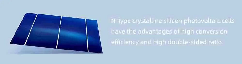
Compared with the traditional P-type single crystal battery and P-type polycrystalline battery, N-type crystalline silicon photovoltaic cells have the advantages of high conversion efficiency, high double-sided ratio, low temperature coefficient, no light attenuation, good weak light effect, and longer carrier life.
TOPCon
TOPCon (Tunnel Oxide Passivated Contact) – passivation contact of oxide layer. There is no essential difference between the front side and the conventional N-type solar cell or N-PERT solar cell. The core technology of the crystalline silicon photovoltaic cells is the passive contact of the back side. There are the top 10 TOPCon solar cell manufacturers in China
The back of the battery is composed of an ultra-thin silicon oxide (1~2nm) and a phosphorus doped microcrystalline amorphous mixed Si film, which together form a passive contact structure. The passivation property is activated by the annealing process, during which the crystallinity of Si films changes from microcrystalline amorphous mixed phase to polycrystalline. Annealing at 850 ° C, iVoc>710mV, J0 at 9-13fA/cm2, shows excellent passivation performance of passive contact structure.
The structure can prevent minority carrier hole recombination and improve the open circuit voltage and short circuit current of the crystalline silicon photovoltaic cells. The ultra-thin oxide layer can enable many electrons to tunnel into the polycrystalline silicon layer while blocking the recombination of minority carrier holes.
The excellent passivation effect of ultra-thin silicon oxide and heavily doped silicon film makes the energy band on the silicon surface bend, thus forming a field passivation effect. The probability of electron tunneling is greatly increased, the contact resistance is reduced, and the open circuit voltage and short circuit current of the crystalline silicon photovoltaic cells are improved, thus improving the conversion efficiency of the battery.
HJT
HJT (Heterojunction with Intrinsic Thin film) – Intrinsic thin film heterojunction battery. The battery produced by HJT solar cell manufacturers has a symmetrical double-sided battery structure, with N-type crystalline silicon in the middle. Intrinsic amorphous silicon films and P-type amorphous silicon films are deposited successively on the front side to form P-N junctions.
On the back side, the intrinsic amorphous silicon film and N-type amorphous silicon film are deposited successively to form the back surface field. In view of the poor conductivity of amorphous silicon, transparent conductive films (TCO) were deposited on both sides of the battery to conduct electricity, and finally screen printing technology was used to form double-sided electrodes.
 It is mainly due to the double passivation effect of N-type silicon substrate and amorphous silicon on substrate surface defects. At present, the mass production efficiency is generally more than 24%;
More than 25% of the technical route has been very clear, that is, using doped nanocrystalline silicon, doped microcrystalline silicon, doped microcrystalline silicon oxide, and doped microcrystalline silicon carbide to replace the existing doping on the front and rear surfaces; HJT crystalline silicon photovoltaic cells may increase the conversion efficiency of superimposed IBC and perovskite to more than 30% in the future.
Since the HJT crystalline silicon photovoltaic cells substrate is usually N-type monocrystalline silicon, and N-type monocrystalline silicon is phosphorus doped, there is no boron oxygen recombination, boron iron recombination, etc. in P-type crystalline silicon, so HJT are immune to LID effect.
The surface of HJT crystalline silicon photovoltaic cells is deposited with TCO film, without insulating layer, so there is no chance to charge the surface layer, and PID can be avoided structurally. The HJT attenuate 1-2% in the first year, and 0.25% annually thereafter, which is far lower than the attenuation of the gallium doped sheet of the PERC battery (2% in the first year, and 0.45% annually thereafter).
Therefore, the power generation per W of the HJT battery in its full life cycle is about 1.9% – 2.9% higher than that of the double-sided PERC crystalline silicon photovoltaic cells.
IBC
IBC (Interdigitated Back Contact) – interdigitated back contact battery technology. The P/N junction, the contact electrode of the substrate and the emission area are made on the back of the crystalline silicon photovoltaic cells in an interdigital shape. There are the top 10 IBC solar cell manufacturers in China.
Core technology: how to prepare p and n regions with good quality and interdigital spacing on the back of the crystalline silicon photovoltaic cells. By printing a interdigital diffusion mask layer containing boron on the back of the battery, the boron on the mask layer diffuses into the N-type substrate to form a p+area, while the area without the mask layer is diffused by phosphorus to form a n+area.
 The front surface is made of pyramidal texture to enhance light absorption, and a front surface field (FSF) is formed on the front surface. The use of ion implantation technology can obtain p and n regions with good uniformity and accurate and controllable junction depth.
The front of the cell is not shielded by grid lines, which can eliminate the loss of light shielding current of metal electrodes, maximize the use of incident photons, and increase the short circuit current by about 7% compared with conventional solar cells.
Because of the back contact structure, it is unnecessary to consider the grid line shielding problem, and the grid line proportion can be appropriately widened, thereby reducing the series resistance and having a high filling factor; It can optimize the design of surface passivation and surface trapping structure, and obtain lower front surface recombination rate and surface reflection, thus improving Voc and Jsc.
Beautiful appearance, especially suitable for photovoltaic building integration; However, the cost of IBC crystalline silicon photovoltaic cells are relatively high and has not yet been industrialized. The manufacturing process of IBC is complex. The cost of IBC battery is almost twice that of conventional battery due to the repeated use of semiconductor technologies such as mask and photolithography.
P-IBC
The P-IBC crystalline silicon photovoltaic cells technology started to attract more attention after Longji came out. Longji’s P-IBC crystalline silicon photovoltaic cells technology is HPBC based on P-type silicon chip. In fact, TNO publicized P-type IBC structure as early as 16-17. P-IBC adds an LPCVD and the others are compatible with PERC.
The laser is a little different, 90% compatible. P-IBC back knot structure has advantages in efficiency. At present, it is still biased towards single side, and the double side rate is less than 50%. It is positioned as a fabric product. The opportunity cost of P-IBC is close to that of PERC, and the efficiency is 24.5% – 25%, achieving a cost gap of 1-3 cents/W.