Solar energy is an inexhaustible renewable and clean energy for mankind. Photovoltaic (PV) technology, which directly converts the sun’s light energy into electricity, the converted electric energy is stored in the lithium ion solar battery, usually use 51.2V 200Ah lithium ion battery and then can be used by home appliances through the inverter, is a major player in the sustainable energy transition to a low-carbon emission society.
Although several materials can and have been used to make solar cells, the vast majority of silicon photovoltaic modules today are dominated by crystalline silicon (c-Si), as silicon is the most abundant element in the earth’s crust after oxygen.
However, energy-intensive c-Si silicon photovoltaic is expensive. Huge advances in the manufacturing chain in the past have made silicon carbide an important low-cost source of electricity.
In 2020, more than 125GW of c-Si modules were installed globally, and more than 700 GW have been installed cumulatively, accounting for 95% of the entire silicon photovoltaic market.
It is estimated that in 20 or 30 years, c-Si silicon photovoltaic could become the most important source of electricity in the world.
Glimpse of the results
Recently, Professor Christophe Ballif of the Swiss Federal Institute of Technology in Lausanne outlined the major changes related to the material and industrial processing of silicon photovoltaic modules.
The cost of single crystal wafers has been reduced due to the dramatic reduction in the cost of polysilicon and the extensive use of diamond wire saws. The concentration of impurities and electronic defects in various types of wafers is also reduced, enabling efficient production of industrial equipment.
Increased automation of tooling, improved line cleanliness, improved cell structure and production technology have all contributed to increasing the efficiency of mainstream modules.
With the introduction of advanced assembly technology and the increase in wafer size, the corresponding device efficiency has been greatly improved. These improvements reduce unit-to-module efficiency losses and will accelerate annual efficiency gains for mainstream modules.
Finally, it also discusses how other photovoltaic technologies can compete with silicon photovoltaic in the mass market.
Core innovation
In the past three decades, the silicon photovoltaic industry has gone from being a treasure in the energy field to being the “new king of electricity”. silicon photovoltaic will play a central role in decarbonizing the global energy economy and mitigating climate change, and silicon photovoltaic technology will continue to be a key player for decades to come.
Data overview
From polysilicon raw materials to wafers
For high-efficiency silicon photovoltaic cells and modules, silicon crystals with low impurity concentrations and few crystal defects are required. Silicon processing begins with metallurgical grade silicon (containing ~1% impurities), which reacts with HCl to form trichlorosilane (TCS), a liquid with a boiling point of 32 °C. TCS with a purity of 9N to 12N was obtained through a series of distillation cycles.
Subsequently, the TCS is fed together with H2 into a cooled stave reactor, where high-purity silicon filaments (several millimeters wide) are heated to 1150 °C. TCS thermally dissociates on the surface of hot silicon filaments, and silicon deposition thickens the filaments into silicon rods 10–20 cm in diameter. The silicon rods are then crushed into blocks and used for the growth of silicon ingots.
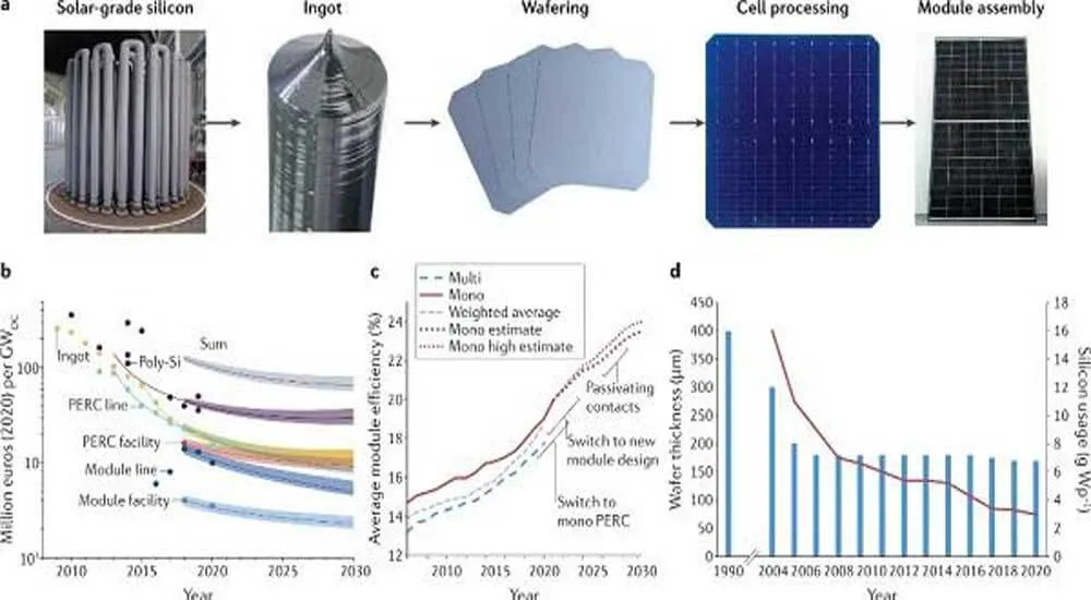
From virgin silicon to silicon photovoltaic solar modules
(a) The main steps of making silicon photovoltaic modules: preparation of purified polysilicon, casting or drawing of ingots, fabrication of wafers, processing of solar cells and assembly of modules.
(b) the learning curve of capital expenditures along the value chain from polysilicon purification of silicon to silicon photovoltaic modules module assembly.
(c) Average efficiency change for mono- and poly-silicon mainstream modules, taking into account all modules sold in the silicon photovoltaic market.
(d) Wafer thickness and Silicon in silicon photovoltaic consumption decrease over time.
Carrier lifetime in silicon
(1) Improve the effective life during silicon photovoltaic modules processing
During silicon photovoltaic solar cell processing, the defect density within a wafer can change significantly. Depending on the processing temperature, precipitates can dissolve or form, depending on their solubility and diffusivity, and the absorption process can remove transition metals by attracting and collecting them to those with higher solubility.
(2) Batch life degradation phenomenon
The carrier lifetime at the end of the solar cell manufacturing process is important, but not sufficient to ensure lasting and efficient solar energy production.
Defect generation in Silicon as a function of light and temperature
(a) Measurement of the spatially resolved effective carrier lifetime (τeff) of p-type 5 × 5 cm-2 polysilicon at 75 °C and “1 sun” illumination using time-resolved photoluminescence imaging;
(b) Maximum equivalent defect concentration N*max during degradation experiments using SiNx:H-coated Cz and FZ wafers.
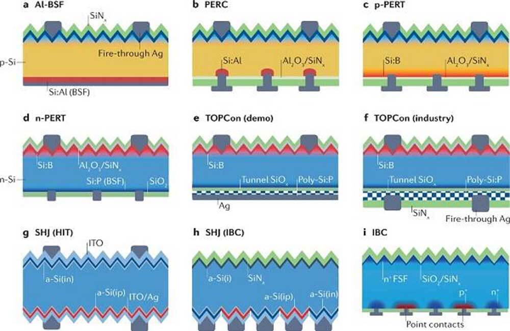
Schematic of a typical solar cell structure
(a) A simple cell design based on p-type silicon, where phosphorus diffuses to form a highly n+ doped front side and a full-area Al back contact forms a highly p+ doped back side, which is called an aluminum back field cell (Al-BSF).
(b) Local back contacts in passivated emitter and back cell (PERC) structures.
(c–d) Local contacts are also used to passivate the emitter and fully post diffusion (PERT) cells, a design suitable for both p-type and n-type wafers.
(e-f) n-type cells designed with tunnel oxide passivated contacts (TOPCon), either with evaporated silver contacts used in R&D or with localized laser ablation introduced in industry.
(g) Silicon in silicon photovoltaic heterojunction (SHJ) design, also known as heterojunction with inherently thin layers (HIT).
(h) SHJ for back contact using interdigitated back contact (IBC);
(i) IBC design with n+-doped front surface field (FSF) and post-diffusion contacts.
Solar cell technology in silicon photovoltaic
(1) Al-BSF battery process
Schematic process flow for fabricating solar cells using different structures
In most passivated emitters and back cells (PERCs) “selective” emitters are created by adding a third step after phosphorous diffusion, where phosphorous glass and crystalline silicon surfaces are laser fused to print metal later Highly doped regions are created in the regions of the fingers.
(2)Development to PERC and other designs
Typical performance characteristics of crystalline silicon solar cells
(a) External quantum efficiency (solid symbols) and reflectivity (open symbols) of Al-BSF and PERC solar cells.
(b) C-V curves of PERC cells.
High temperature passivation contact
In PERC and PERT solar cells, the metal locally contacts the silicon on both sides. This results in significant recombination, limiting the open circuit voltage. This issue has sparked interest in developing passivated contacts, which consist of a stack of layers that suppress surface defects in silicon, but ensure selective charge collection to metal electrodes.
Low temperature passivation contact
Another route to form passivated contacts relies on hydrogenated amorphous silicon (a-Si:H). In all methods involving a-Si:H, post-processing steps must be kept below 200–250 °C: hydrogen evolution at temperatures above 200 °C results in performance degradation (mainly through passivation losses).
This effect can be mitigated or even reversed to temperatures as high as 400 °C, but above 450 °C, the passivation ability of a-Si:H is continuously lost. Therefore, silver screen printing pastes cannot be sintered at high temperatures like standard cell processing, but require the use of low curing temperature pastes.
Minimize unit-to-module losses
Moving from a single wafer to a complete module, there is a systematic difference between the module power and the sum of the individual cell powers, the ratio of these powers is called the cell-to-module (CTM) power ratio, which is typically around 95-97%. Also, the module efficiency is lower than the average cell efficiency, resulting in a CTM efficiency ratio of typically 85-90%.
Continuous industry improvement
Average module efficiency is increasing at an absolute rate of about 0.3-0.4% per year, and this trend is increasing with the transition to single silicon and new module designs. Efficiency gains will continue over the next decade, and finally, through the series of improvements described, the maximum practical efficiency of single-junction silicon modules should be reached (23-24% for mainstream modules, possibly 25% for high-end modules).
Alternative technologies to silicon
Silicon photovoltaic dominates the silicon photovoltaic industry, with a market share of close to 95% in 2020, with a well-established supply chain and standardized designs. While other PV technologies have potential advantages (such as reducing material use of thin films), capturing a smaller market share is a big challenge for them because they have to show better price or efficiency than silicon, at least the same reliability.
From unit to module
(a) A typical unit-to-module loss analysis using the modeling package SmartCalc.CTM;
(b) the evolution of standard module designs from 2000 to 2021;
(c) The silicon photovoltaic modules are assembled in series by half-cut cells.
Achievement inspiration
Silicon photovoltaic, with an impressive pace of development in terms of cost reduction, have improved stable efficiencies at the cell and module level for commercial products. Much R&D is continuing to further improve silicon materials and reduce their cost by improving current industry standard processes or developing low-cost methods and hardware, as well as improving cell manufacturing to enable next-generation products containing passivated contacts.
Combined with improvements in module technology (larger area, half-cell, tile ribbon, ribbon cell, multifilament, reverse contact methods), this will ensure further reduction of the efficiency gap between today’s record-setting laboratory silicon photovoltaic c-Si solar cells.
Due to the area-related system cost, a higher-efficiency approach can be achieved by combining silicon with a higher-bandgap top cell, where perovskites are prime candidates for absorbers. Even at the TW scale, silicon PV devices can be fabricated without any scarce materials, and alternative materials can be used for key elements.
The space for solar power generation (long-distance transport, electrochemical storage) and its conversion to heat, cold or chemicals such as through electricity to natural gas (H2, NH3, etc.) is economically sustainable.
As the International Energy Agency puts it, the silicon photovoltaic industry has gone from an energy gem to a “new king of electricity” over the past three decades. silicon photovoltaic will play a central role in decarbonizing the global energy economy and mitigating climate change, and silicon photovoltaic technology will continue to play a key role in the coming decades.
We offer lithium ion battery products, solutions, and services across the entire energy value chain. We support our customers on their way to a more sustainable future.


 (a) The main steps of making silicon photovoltaic modules: preparation of purified polysilicon, casting or drawing of ingots, fabrication of wafers, processing of solar cells and assembly of modules.
(b) the learning curve of capital expenditures along the value chain from polysilicon purification of silicon to silicon photovoltaic modules module assembly.
(c) Average efficiency change for mono- and poly-silicon mainstream modules, taking into account all modules sold in the silicon photovoltaic market.
(d) Wafer thickness and Silicon in silicon photovoltaic consumption decrease over time.
(a) The main steps of making silicon photovoltaic modules: preparation of purified polysilicon, casting or drawing of ingots, fabrication of wafers, processing of solar cells and assembly of modules.
(b) the learning curve of capital expenditures along the value chain from polysilicon purification of silicon to silicon photovoltaic modules module assembly.
(c) Average efficiency change for mono- and poly-silicon mainstream modules, taking into account all modules sold in the silicon photovoltaic market.
(d) Wafer thickness and Silicon in silicon photovoltaic consumption decrease over time.
 (a) Measurement of the spatially resolved effective carrier lifetime (τeff) of p-type 5 × 5 cm-2 polysilicon at 75 °C and “1 sun” illumination using time-resolved photoluminescence imaging;
(b) Maximum equivalent defect concentration N*max during degradation experiments using SiNx:H-coated Cz and FZ wafers.
Schematic of a typical solar cell structure
(a) Measurement of the spatially resolved effective carrier lifetime (τeff) of p-type 5 × 5 cm-2 polysilicon at 75 °C and “1 sun” illumination using time-resolved photoluminescence imaging;
(b) Maximum equivalent defect concentration N*max during degradation experiments using SiNx:H-coated Cz and FZ wafers.
Schematic of a typical solar cell structure
 (a) A simple cell design based on p-type silicon, where phosphorus diffuses to form a highly n+ doped front side and a full-area Al back contact forms a highly p+ doped back side, which is called an aluminum back field cell (Al-BSF).
(b) Local back contacts in passivated emitter and back cell (PERC) structures.
(c–d) Local contacts are also used to passivate the emitter and fully post diffusion (PERT) cells, a design suitable for both p-type and n-type wafers.
(e-f) n-type cells designed with tunnel oxide passivated contacts (TOPCon), either with evaporated silver contacts used in R&D or with localized laser ablation introduced in industry.
(g) Silicon in silicon photovoltaic heterojunction (SHJ) design, also known as heterojunction with inherently thin layers (HIT).
(h) SHJ for back contact using interdigitated back contact (IBC);
(i) IBC design with n+-doped front surface field (FSF) and post-diffusion contacts.
(a) A simple cell design based on p-type silicon, where phosphorus diffuses to form a highly n+ doped front side and a full-area Al back contact forms a highly p+ doped back side, which is called an aluminum back field cell (Al-BSF).
(b) Local back contacts in passivated emitter and back cell (PERC) structures.
(c–d) Local contacts are also used to passivate the emitter and fully post diffusion (PERT) cells, a design suitable for both p-type and n-type wafers.
(e-f) n-type cells designed with tunnel oxide passivated contacts (TOPCon), either with evaporated silver contacts used in R&D or with localized laser ablation introduced in industry.
(g) Silicon in silicon photovoltaic heterojunction (SHJ) design, also known as heterojunction with inherently thin layers (HIT).
(h) SHJ for back contact using interdigitated back contact (IBC);
(i) IBC design with n+-doped front surface field (FSF) and post-diffusion contacts.
 In most passivated emitters and back cells (PERCs) “selective” emitters are created by adding a third step after phosphorous diffusion, where phosphorous glass and crystalline silicon surfaces are laser fused to print metal later Highly doped regions are created in the regions of the fingers.
(2)Development to PERC and other designs
Typical performance characteristics of crystalline silicon solar cells
In most passivated emitters and back cells (PERCs) “selective” emitters are created by adding a third step after phosphorous diffusion, where phosphorous glass and crystalline silicon surfaces are laser fused to print metal later Highly doped regions are created in the regions of the fingers.
(2)Development to PERC and other designs
Typical performance characteristics of crystalline silicon solar cells
 (a) External quantum efficiency (solid symbols) and reflectivity (open symbols) of Al-BSF and PERC solar cells.
(b) C-V curves of PERC cells.
(a) External quantum efficiency (solid symbols) and reflectivity (open symbols) of Al-BSF and PERC solar cells.
(b) C-V curves of PERC cells.

 (a) A typical unit-to-module loss analysis using the modeling package SmartCalc.CTM;
(b) the evolution of standard module designs from 2000 to 2021;
(c) The silicon photovoltaic modules are assembled in series by half-cut cells.
(a) A typical unit-to-module loss analysis using the modeling package SmartCalc.CTM;
(b) the evolution of standard module designs from 2000 to 2021;
(c) The silicon photovoltaic modules are assembled in series by half-cut cells.
 Due to the area-related system cost, a higher-efficiency approach can be achieved by combining silicon with a higher-bandgap top cell, where perovskites are prime candidates for absorbers. Even at the TW scale, silicon PV devices can be fabricated without any scarce materials, and alternative materials can be used for key elements.
The space for solar power generation (long-distance transport, electrochemical storage) and its conversion to heat, cold or chemicals such as through electricity to natural gas (H2, NH3, etc.) is economically sustainable.
As the International Energy Agency puts it, the silicon photovoltaic industry has gone from an energy gem to a “new king of electricity” over the past three decades. silicon photovoltaic will play a central role in decarbonizing the global energy economy and mitigating climate change, and silicon photovoltaic technology will continue to play a key role in the coming decades.
Due to the area-related system cost, a higher-efficiency approach can be achieved by combining silicon with a higher-bandgap top cell, where perovskites are prime candidates for absorbers. Even at the TW scale, silicon PV devices can be fabricated without any scarce materials, and alternative materials can be used for key elements.
The space for solar power generation (long-distance transport, electrochemical storage) and its conversion to heat, cold or chemicals such as through electricity to natural gas (H2, NH3, etc.) is economically sustainable.
As the International Energy Agency puts it, the silicon photovoltaic industry has gone from an energy gem to a “new king of electricity” over the past three decades. silicon photovoltaic will play a central role in decarbonizing the global energy economy and mitigating climate change, and silicon photovoltaic technology will continue to play a key role in the coming decades.